Corporate profile
Company name
Toho Koki Seisakusho Co., Ltd.
Address
38 Kogane-cho, Yokkaichi City, Mie Prefecture 512-8062
Telephone
FAX
(+81)-59-365-4383
President
Eisuke Suzuki
Businesses
Manufacture and sale of next generation semi-conductor substrate planarization machines (CARE equipment)
CMP (Chemical Mechanical Polishing) pads business, Machining of large machine parts
Business hours
8:20~17:00(Japan time)
Holidays
Saturday, Sunday, Holidays
Capital
80 million yen
Established
‘July 3, 1956
History
1958
Built factory in Oinokawa, Yokkaichi City. Started design, manufacture and installation of chemical machinery.
1967
Joined the Yokkaichi Machinery and Metalworking Industrial Complex Cooperative Association and built the factory that is currently our head office.
1982
Increased capital to 50 million yen. Began full-scale introduction of numerical-control (NC) machine tools.
1986
Established Toho Engineering Co., Ltd. Entered semiconductor field.
2000
Launched sales of the CMP series of CMP pad groove processing machines.
2002
Began collaborative research on CMP pads with Professor Doi of Saitama University.
2004
Invested in Araca Incorporated (a U.S. company). Launched CMP services business.
2008
Collaborative research on TSV-CMP with Professor Chen of the National Taiwan University of Science and Technology
2009
Participated in research into the CARE method invented by Professor Kazuto Yamauchi and Assistant Professor Yasuhisa Sano at Osaka University.
2011
Launched the Saisei Eco-Cap® for attaching and detaching abrasive pads
2012
Selected by the Ministry of Economy, Trade and Industry (METI) under their innovation hub location project. (Development of equipment for the evaluation of polishing pads for the CARE method)
Conducted joint research with the Technology Research Institute (CEA-Leti) at the French Alternative Energies and Atomic Energy Commission (CEA) on polishing pad regeneration technology.
2013
Selected for the Strategic Core Technology Advancement Project (Development of basic technologies for the CARE method)
2014
Launched sales of the INS series of pad groove inspection devices。
2015
Selected by the New Energy and Industrial Technology Development Organization (NEDO) for its project to promote cooperation in the creation of innovative manufacturing industries (Development of CARE method elemental technologies for commercialization.)
2018
Delivered the first experimental device CARE-TEC® to Nagoya University
Selected for the Strategic Core Technology Advancement Project (development of applied technology for CARE)
Started collaborative development on the AIN template with Dr. Hideto Miyake, Professor at Mie University.
2021
Selected for the Strategic Core Technology Advancement Project (development of AIN template), Toho Koki absorbs Toho Engineering in a merger.
Increased capital to 80 million yen.
2022
Completed construction of a new clean room (450 m2) for semiconductor substrate production
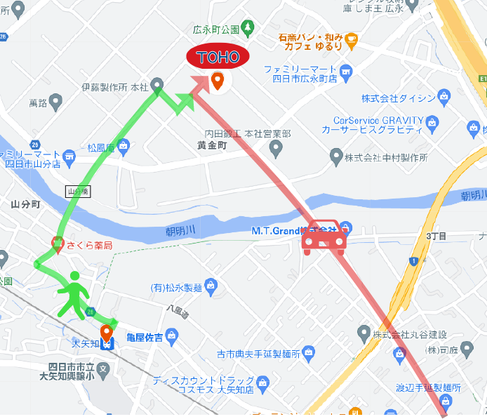
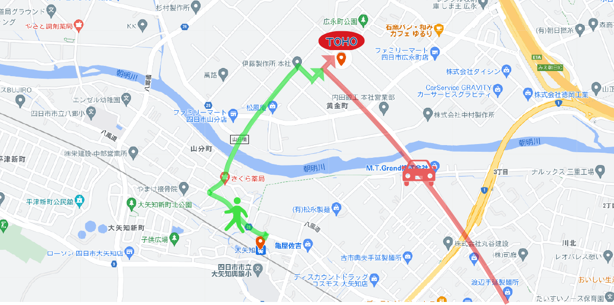
Access
By car
Exit at Yokkaichi Higashi IC on the Higashi-Meihan Expressway and turn right at the first traffic light, turn left at the fourth traffic light, turn left at the third traffic light on the Hokusei Bypass, cross the Hironaga Bridge to Kogane-cho.
By train
From Tomida Station on the Kintetsu-Nagoya Line go to Tomida Station of the Sangi Railway Line, take a train bound for Hobo or Nishi Fujiwara and get off at Oyachi Station. It is a 15-minute walk from the station.
By taxi
Take a taxi from Tomida Station on the Kintetsu-Nagoya Line.
Greetings from the President
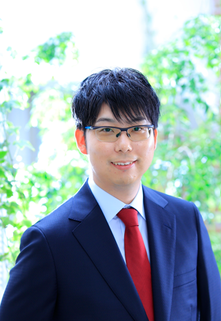
Eisuke Suzuki
Toho Koki Seisakusho contributes to society through the development of new markets for our innovative products. The shift to electric vehicles (EVs) is currently attracting a lot of attention, and semiconductors that efficiently convert electricity are critical.
Our company provides a solution to this issue through our extreme planarization technology for next-generation semiconductor substrates.
We have delivered our first experimental device to Nagoya University and aim to further promote the utilization of this technology through collaboration with other corporations.